- 您现在的位置:买卖IC网 > Sheet目录2000 > ISL12008IB8Z (Intersil)IC RTC I2C LO-POWER 8-SOIC
2
FN6690.1
September 26, 2008
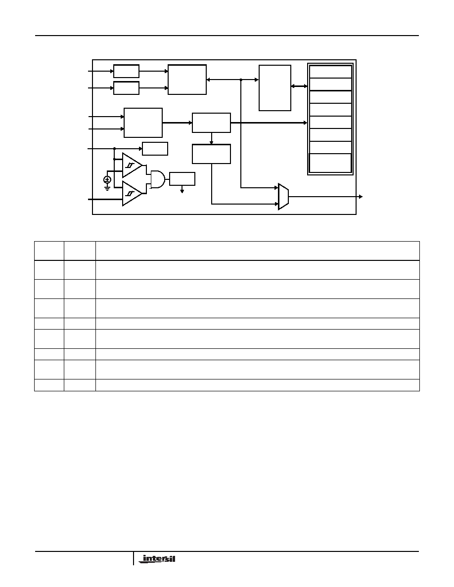
Block Diagram
I2C
INTERFACE
RTC
CONTROL
LOGIC
FREQUENCY
OUT
RTC
DIVIDER
SDA
BUFFER
CRYSTAL
OSCILLATOR
POR
SWITCH
SCL
BUFFER
SDA
SCL
X1
X2
VDD
VBAT
FT/OUT
INTERNAL
SUPPLY
VTRIP
SECONDS
MINUTES
HOURS
DAY OF WEEK
DATE
MONTH
YEAR
CONTROL
REGISTERS
Pin Descriptions
PIN
NUMBER SYMBOL
DESCRIPTION
1
X1
The X1 pin is the input of an inverting amplifier and is intended to be connected to one pin of an external 32.768kHz quartz
crystal. X1 can also be driven directly from a 32.768kHz source.
2
X2
The X2 pin is the output of an inverting amplifier and is intended to be connected to one pin of an external 32.768kHz quartz
crystal.
3VBAT
This input provides a backup supply voltage to the device. VBAT supplies power to the device in the event that the VDD supply
fails. This pin should be tied to ground if not used.
4
GND
Ground
5
SDA
Serial Data (SDA) is a bidirectional pin used to transfer serial data into and out of the device. It has an open drain output and
may be wire OR’ed with other open drain or open collector outputs.
6
SCL
The Serial Clock (SCL) input is used to clock all serial data into and out of the device.
7
FT/OUT
512Hz Frequency Output or digital output pin. The function is set via the configuration register. This pin is open drain and
requires an external pull-up resistor.
8VDD
Power supply
ISL12008
发布紧急采购,3分钟左右您将得到回复。
相关PDF资料
ISL12020MIRZ-T7A
IC RTC/CALENDAR TEMP SNSR 20DFN
ISL12022IBZ-T7A
IC RTC/CALENDAR TEMP SNSR 8SOIC
ISL12022MAIBZ
IC RTC/CALENDAR TEMP SNSR 20SOIC
ISL12022MIBZ-T7A
IC RTC/CALENDAR TEMP SNSR 20SOIC
ISL12022MIBZR5421
IC RTC/CALENDAR TEMP SNSR 20SOIC
ISL12023IVZ
IC RTC/CLDR TEMP SNSR 14-TSSOP
ISL12024IRTCZ
IC RTC/CALENDER 64BIT 8-TDFN
ISL12024IVZ
IC RTC/CALENDAR EEPROM 8-TSSOP
相关代理商/技术参数
ISL12008IB8Z-T
功能描述:实时时钟 LW PWR RTC W/RESEAL 8LD RoHS:否 制造商:Microchip Technology 功能:Clock, Calendar. Alarm RTC 总线接口:I2C 日期格式:DW:DM:M:Y 时间格式:HH:MM:SS RTC 存储容量:64 B 电源电压-最大:5.5 V 电源电压-最小:1.8 V 最大工作温度:+ 85 C 最小工作温度: 安装风格:Through Hole 封装 / 箱体:PDIP-8 封装:Tube
ISL12020
制造商:INTERSIL 制造商全称:Intersil Corporation 功能描述:Low Power RTC with VDD Battery Backed SRAM and Embedded Temp Compensation 【5ppm with Auto Day Light Saving
ISL12020CBZ
制造商:Rochester Electronics LLC 功能描述: 制造商:Intersil Corporation 功能描述:
ISL12020IBZ
制造商:INTERSIL 制造商全称:Intersil Corporation 功能描述:Low Power RTC with VDD Battery Backed SRAM and Embedded Temp Compensation 【5ppm with Auto Day Light Saving
ISL12020M
制造商:INTERSIL 制造商全称:Intersil Corporation 功能描述:Low Power RTC with Battery Backed SRAM, Integrated ±5ppm Temperature Compensation and Auto Daylight Saving
ISL12020M_11
制造商:INTERSIL 制造商全称:Intersil Corporation 功能描述:High-Accuracy RTC Modules, Feature-Rich RTCs
ISL12020MIRZ
功能描述:实时时钟 REAL TIME CLOCK AND TMP COMP CRYSTL INLD RoHS:否 制造商:Microchip Technology 功能:Clock, Calendar. Alarm RTC 总线接口:I2C 日期格式:DW:DM:M:Y 时间格式:HH:MM:SS RTC 存储容量:64 B 电源电压-最大:5.5 V 电源电压-最小:1.8 V 最大工作温度:+ 85 C 最小工作温度: 安装风格:Through Hole 封装 / 箱体:PDIP-8 封装:Tube
ISL12020MIRZ-EVALZ
功能描述:电源管理IC开发工具 ISL12020MIRZ-EVALZ EVALBRD ROHS COMPL
RoHS:否 制造商:Maxim Integrated 产品:Evaluation Kits 类型:Battery Management 工具用于评估:MAX17710GB 输入电压: 输出电压:1.8 V